3.2 H8/3048 Overview

  In this course, an H8/3048 is used as the sample processor from the H8/300H family.The H8/3048 includes the following three types: one having a mask ROM or OTPROM as an internal ROM (simply referred to as the H8/3048), an H8/3048F having an internal writable flash memory with two power supplies (5V and 12V) and an H8/3048F-ONE having an internal writable flash memory with a single power supply (5V). The only difference among them is the type of internal ROM, the rest are almost the same. Although this chapter describes the overview of the H8/3048F-ONE, the descriptions in this and following chapters are common to all types. Note, however, that the training board has been developed based on the H8/3048F-ONE.
Figure 3.3 shows the H8/3048F-ONE internal block.
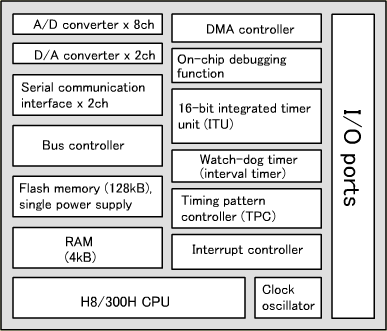
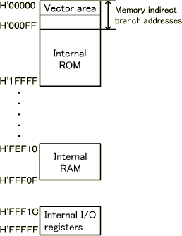
Figure 3.3: H8/3048F-ONE Internal Block

Features of CPU

- 16-bit CPU which serves as a general-purpose register machine.
  Equipped with 16-bit × 16 general-purpose registers.
(Also available in 8-bit × 16 + 16-bit × 8 or 32-bit × 8 form.)

- High-speed CPU.
  The maximum operating frequency of the H8/3048F-ONE is 25MHz and addition/subtraction can be executed in 80ns and multiplication/division in 560ns.
  The CPU is operated based on clock signals and the higher the clock signal frequency, the faster the operation. The time of one 25MHz clock signal pulse is 0.04 microsecond (40ns), which is called "1 state". Addition/subtraction are completed in two states and multiplication/division in 14 states.

- Equipped with a maximum 16M bytes of address space.
(CPU, instructions and programs are described in Chapters 4, 5 and 6.)

Available both as single-chip and multi-chip microcomputer
  It can be used as a single-chip microcomputer thanks to the internal ROM, RAM and data I/O functions in addition to the CPU.
  It can also be used as a multi-chip microcomputer when an external memory is added due to insufficient ROM or RAM capacity. When used as a multi-chip microcomputer, it has 24 address pins and up to 16M bytes of memory can be added.Addresses consume 16M, 8 bits per address. Since there are 16 data pins, 16 bits can be read or written simultaneously.

Internal ROM
  It has a 128k byte, writable flash memory with a single 5V power supply. This enables onboard writing.
For writing to the flash memory, a boot mode using a serial interface is supported. Writing with a user-defined program is also available.

Internal RAM
It has an internal, 4k byte RAM.

I/O ports: 70 I/O pins and 8 input-only pins
  The I/O ports can be used to input switch on/off statuses or signals from various sensors. When used as output ports, they can control blinking of a display lamp or turn a motor or heater on and off. The I/O ports are widely used as general-purpose I/O functions.
  On the training board, they are used to read switch statuses and control LED displays.

Internal SCI (serial communication interface) × 2 channels
  Channel 0 is available for a smart card interface.
For start-stop synchronization, it is used for RS-232C and other communication functions. It is connected to a PC to enable data exchange.
  On the training board, it is connected to a PC via RS-232C to send a created program from a PC to the board or input a command for debugging.

Internal ITU (integrated timer unit) composed of 16-bit timer × 5 channels
  Pulse outputs from up to 12 pins and up to 10 types of pulse inputs can be processed.
  It has a wide variety of uses such as measurement of time, speed and frequency as well as control of pulse motors.
  On the training board, a piezoelectric buzzer is provided so that pulses can be heard as sounds.

Internal TPC (programmable timing pattern controller)
capable of outputting up to 16-bit pulses using the ITU as a time base
  In combination with the ITU, a large number of pulse outputs are available.

Internal watch-dog timer
  Program runaway can be detected. Since control using a microcomputer is based on programs, an extremely dangerous situation may occur if a program should run away. This function is indispensable for creating a highly reliable system.

Internal A/D converter with 10-bit resolution × 8 channels
The A/D converter is designed to input analog voltages instead of digital voltages.For example, signals from a temperature sensor are input not by high/low digital voltages but analog voltages. These signals are read after being converted into 10-bit binary numbers.
On the training board, 0 to 5V analog voltages can be input with added volume.

Internal 8-bit D/A converter × 2 channels
  Unlike the A/D converter, the D/A converter is designed to output analog voltages. It is also used to output desired waveforms or adjust volume or hue of a TV.
  On the training board, LEDs can be driven with D/A-converted output voltages to control brightness.

Internal DMA controller × 4 channels (max.)
  Used for high-speed data transfer.It enables data to be transferred faster than with the CPU. It is generally used with a timer and other communication functions.

Internal refresh controller
  Refreshing is required to retain the data in the dynamic RAM. This microprocessor has an internal controller for this purpose.


The H8/3048F-ONE can be used as a single-chip microcomputer. In this form, no external memory can be added and only the internal one is available. The operating mode when it is used as a single-chip microcomputer is referred to as "single-chip mode". Figure 3.4 shows the memory map in single-chip mode.In this mode, the memory addresses are expressed with 20 bits (5 digits in hexadecimal notation).

Figure 3.4: Memory Map in Single-chip Mode


The H8/3048F-ONE can also be used as a multi-chip microcomputer. The operating mode in this case is referred to as "external extension mode". In external extension mode, a memory or peripheral IC can be connected externally. Figure 3.5 shows the memory map in external extension mode.
Since there are 24 address buses, up to 16M bytes of external memory can be added. Addresses are expressed with 6-digit, hexadecimal numbers.
The addresses of the internal ROM, RAM and internal I/O register, however, are fixed and cannot be changed. If the address of the memory to be added is the same as that of the internal ROM, RAM or internal I/O register, the internal function has priority, disabling reading/writing from/to the external memory.

Figure 3.5: Memory Map in External Extension Mode


Although this chapter has described the overview of the H8/3048F-ONE, table 3.1 shows the differences between the H8/3048, H8/3048F and H8/3048F-ONE as well as their features for summary.

Table 3.1: Differences Between the H8/3048, H8/3048F and H8/3048F-ONE and Their Features
H8/3048 H8F/3048 H8/3048F-ONE
CPU 16-bit CPU, general-purpose register machine
Maximum operating frequency 18MHz 16MHz 25MHz
Address space 16Mbyte max
Internal ROM Mask ROM/
OTPROM
Flash memory
(writable with 2 power supplies, 5V and 12V)
Flash memory
(writable with single 5V power supply)
128Kbyte
Internal RAM 4Kbyte
Operating mode Available both as single- and multi-chip microcomputer
Power supply voltage Vcc -0.3 to +7.0 (V) -0.3 to +7.0 (V) 5V operation: -0.3 to +7.0 (V)
operation: -0.3 to +4.6 (V)
Peripheral functions   - 78 I/O ports in all: 70 I/O pins and 8 input-only pins
  - SCI x 2 channels
  - ITU composed of 16-bit timer x 5 channels
  - TPC capable of outputting up to 16-bit pulses
  - Watch-dog timer for detecting program runaway
  - A/D converter with 10-bit resolution x 8 channels
  - 8-bit D/A converter x 2 channels
  - DMA controller x 4 channels (max.)
  - Refresh controller