13.7 Connecting CPU to Memory (Connecting EPROM Using 8-bit Data Bus) |
The following conditions are assumed here for connecting a CPU to a memory: CPU: H8/3048F (clock frequency: 10MHz) 16Mbyte memory space (24 address pins) Internal ROM disabled (internal ROM is not used but an EPROM is connected externally) 8-bit data bus (D8 to D15 used) RD, HWR and CS0 to CS7 are used as control signals Memory: HN27C4001G-10 for EPROM (access time: 100ns) HM628512BI-8 for SRAM (access time: 85ns) |
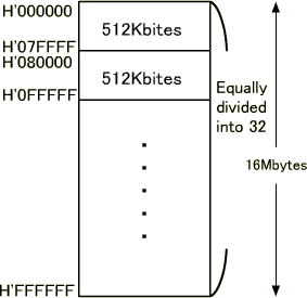
First, let's consider how to connect a CPU to a memory using an 8-bit data bus. Address assignment What should be determined first is to which addresses the memory is to be connected. As described in "Exception Handling", a program operating based on resetting and the reset vector must be located in a ROM. Since the reset vector is between H'000000 and H'00003, a ROM must be connected to starting from the H'000000 address if only one ROM is connected. In internal ROM enable mode, the internal ROM addresses are from H'000000 to H'01FFFF. In internal ROM disable mode, the HN27C4001G must be connected between H'000000 and H'01FFFF. The internal ROM is assumed to be disabled here. Generally, a memory is assigned to one of the spaces obtained by equally dividing the CPU memory space by the memory capacity. Since the CPU memory space is 16Mbytes and the EPROM capacity is 512kbytes, the CPU memory space is divided into 32 equal parts. The smallest addresses are from H'000000 to H'07FFFF. This is shown in Figure 13.11.
|
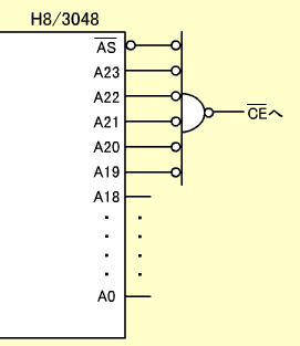
Next, let's develop an address decode circuit. The EPROM should be designed to operate only when the address output by the CPU is the EPROM address (from H'000000 to H'07FFFF) and operation is enabled only when the CE pin of the EPROM is set at low level. The address decode circuit is designed to set CE at low level when the address output by the CPU is the EPROM address. Then, how can you determine that the address output by the CPU is the EPROM address? The EPROM address is represented as follows in binary notation: H'000000: 0000 0000 0000 0000 0000 0000 H'07FFFF: 0000 0111 1111 1111 1111 1111 Accordingly, you can determine that it is the EPROM address when the upper 5 bits (A23 to A19) of the address are all 0. On the other hand, you can determine that the address of the address bus is valid when AS is set at low level. As a result, CE of the EPROM is set at low level under the following conditions: AS is at low level and A23 to A19 are also at low level Figure 13.12 shows a sample circuit to satisfy them.
|
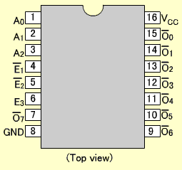
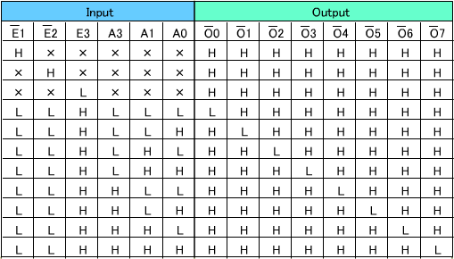
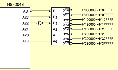
The more memories that are connected, the harder it is to develop decoders as shown above for each memory. By using the HD74AC138, a standard logic IC, you can develop select signals for 8 memories.Figure 13.11 shows the HD74AC138 pin assignment and truth values are shown in Table 13.7.
|
|
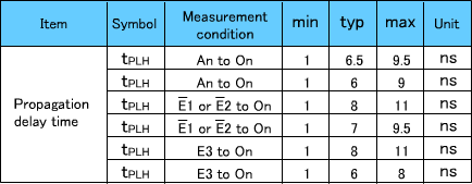
Table 13.8 shows the AC characteristics.
|
A decode circuit using the HD74AC138 is shown in Figure 13.14.
|
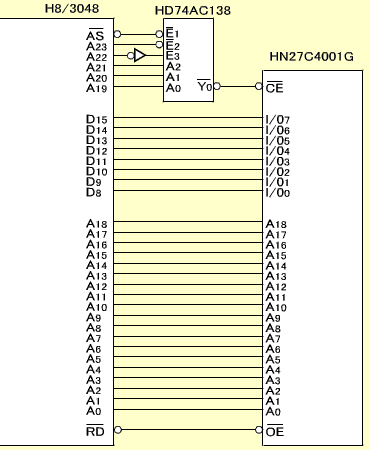
Figure 13.15 shows connection between H8/3048 and HN27C4001G.
|
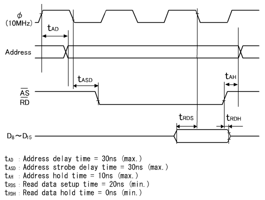
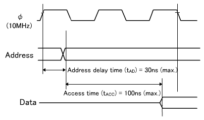
The memory address pins are connected to the corresponding address pins of the CPU (A0 to A0, A1 to A1, etc.) from A0 to A18. The memory data pins are connected to the corresponding data pins of the CPU (I/O0 to D8, I/O1 to D9, etc.) from I/O0 to I/O7, to D8 to D15. Address-decoded signals are input to the memory CE pin. RD signals of the CPU are input to the memory OE pin. When the CPU is in read mode, the RD signal and OE are set at low and reading starts. This completes logical connection between the CPU and the memory. Next, it must be calculated whether the speeds of the CPU and the memory match. Since an EPROM is connected, the CPU read timings are calculated here. Figure 13.16 shows CPU timings required for calculation.
|
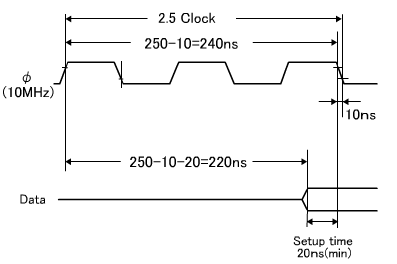
The most important parameters in CPU read timings are read data setup and hold times. Setup time calculation A setup time of 20ns is required for the trailing edge of T3. The time from start of reading to the trailing edge of T3 is obtained as follows by subtracting the clock trailing time (10ns) from 2.5 clocks (250ns):
Since 20ns (min.) is required as the setup time, this requirement is satisfied if data arrive at the CPU 220ns after the start of reading. This is shown in Figure 13.17.
|
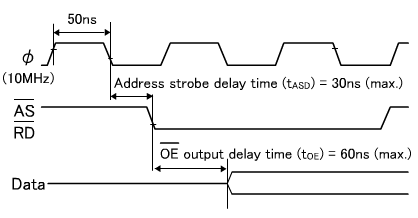
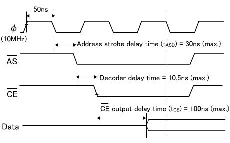
Data are output from the memory only when all the access time, OE output delay time and CE output delay time requirements are satisfied.
|
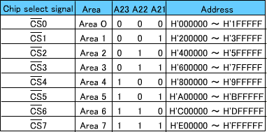
The longest time for data to be output is 190.5ns due to the CE output delay time. As for the setup time, it causes no problem since the calculation results are 190.5ns (max.) against the requirement of 240ns (max.), providing an allowance of about 50ns. Hold time calculation The input data hold time required by the H8/3048F is 0ns (min.) for the address strobe leading edge. In other words, it is acceptable as long as data are not changed before the address strobe leading edge. The following three factors change data in the memory: - An address is changed - CE is set at high level - OE is set at high level An address is changed after the address hold time has passed following the address strobe leading edge.As a result, the hold time of 0ns (min.) is secured. On the other hand, CE is set at high level after the decoder delay time has passed following the address strobe leading edge. As a result, the hold time of 0ns (min.) is also secured. As for OE, RD is used as it is. RD is set at high level at the same time AS is set at high level. The memory outputs data for 0ns (min.) after OE is set at high level. As described above, the hold time of 0ns (min.) is satisfied in all cases. Consequently, you can see that the requirements for both setup and hold times are satisfied regarding EPROM reading. This method has a wide range of uses and can be applied to various connections between the CPU and the memory. The setup time required by the CPU, however, may not be satisfied if the address decoder delay time is long. In addition, the address strobe (AS) is used in the address decode circuit and delayed AS tightens the requirement for the setup time. To simplify a decode circuit, the H8/3048 is provided with signals from CS0 to CS7. These signals are obtained by decoding the upper 3 bits of the CPU addresses. Since 3 bits are decoded, the 16Mbyte memory space is divided into 8 equal parts. These are called area 0 to area 7. When the CPU accesses area 0, CS0 is set at low level. This is shown in Table 13.9.
|
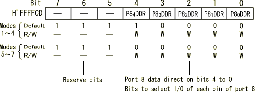
In the case of the H8/3048, the CS0 to CS7 signals are available instead of the AS signals.In this case, 3 bits of addresses need not be decoded. In addition, the CS0 to CS7 signals are output faster than the AS signals and at the same timing as address signals, allowing for setup time and enabling slower memory to be connected. In order to use the CS0 to CS7 signals, you must set the bus controller accordingly. Since CS0 to CS3 are commonly used with port 8, set the corresponding bit of the P8DDR at 1 (output).
CS0, CS1, CS2 and CS3 correspond to P84DDR, P83DDR, P82DDR and P81DDR, respectively, and are switched to chip select pins when 1 is written.In internal ROM disable mode, however, the CS0 pin is set at 1 and enabled by default. The data direction register is a write-only register and thus incapable of reading. This means that the bit handling instruction is not available for it. CS0 to CS3 can be used as chip select signals simply by setting the P8DDR. CS4 to CS7, on the other hand, can be used as chip select signals simply by setting the chip select control register.
CS7E, CS6E, CS5E and CS4E correspond to CS7, CS6, CS5 and CS4, respectively, and are switched to chip select pins when 1 is written. |
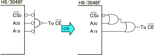
Since the EPROM is connected to the H'000000 address, it is assigned as area 0 and uses CS0.If CS0 is L and both A20 and A19 are 0, it is the EPROM address. Figure 13.23 shows a decode circuit using CS0. |