 |
|
|
|
|

During the “design /
mask creation” phase,
the function of the IC is defined, the
electric circuit is designed, and a mask for IC manufacturing is
created based on the design. |
 |
 |

During the front-end processing phase,
an IC is created on a silicon
substrate (referred to as a “wafer”). |
 |
|

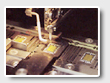
During the back-end processing phase,
the IC chips created during the front-end processing
phase are encapsulated into packages, and thoroughly
inspected before becoming completed products. |
|
 |
|
|
|
|
 |

This procedure is used for the formation
of a circuit pattern during various
front-end processes. |
|
|
|
 |

A device insulation layer (field oxide-film) is
formed for electrical isolation of the
devices.
|
|
|
|
|
|

Transistors are formed in the active regions to control the flow of electrons.
|
|
|
|
 |
|

Devices, such as transistors, are interconnected to form an electronic circuit.
|
|
|
This site guides you through
the manufacturing process with
narrations and Flash
animations.
• The narrations can be turned OFF.
• This site requires the lastest version
of Macromedia
Flash Player.

|

