The HN27C4001G is used here as an EPROM example.
The HN27C4001G has a 4Mbit capacity and 524288 word × 8 bit configuration. Figure 13.6 shows the pin assignment.
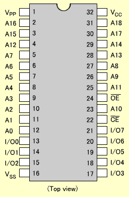 |
| Figure 13.6: NH27C4001G Pin Assignment Diagram |
| 13.5 Sample Memory (EPROM) The HN27C4001G is used here as an EPROM example. The HN27C4001G has a 4Mbit capacity and 524288 word × 8 bit configuration. Figure 13.6 shows the pin assignment.
|
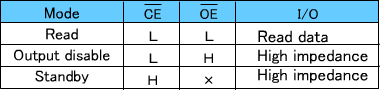
There are 19 address input pins, A0 to A18.Since addresses are input in 19-bit units, this memory has 512-kbyte (to be more precise, 524,288) addresses. The address count of the memory IC is determined by the address pin count. There are 8 data pins, I/O0 to I/O7, meaning that the memory uses 8 bits per address. Since this is a ROM, it is a read only memory when connected to a CPU and the data pins are set to output. They are changed to input pins for writing by an EPROM writer. Here, we consider the case in which it is connected to a CPU and serves as a ROM only. The Vpp pin is designed to apply the write voltage (12V) for writing by an EPROM writer. It is fixed to high or low level for operation as a ROM with connection to a CPU. CE (Chip Enable) is a memory select signal and the memory is selected when it is set at low level. This is used to assign a specific address by adding an address-decoded signal. OE (Output Enable) is an output enable signal and read data is output from a data pin when it is set at low level. The table below summarizes this.
|
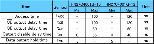
In read mode, the CPU reads data from the EPROM and sets both CE and OE at low level. In output disable mode, the memory is selected but read data is not output to an I/O pin. The I/O pin is set in high impedance mode (disconnected state). In standby mode, the memory is not selected. When CE is set at high level, the system is set in standby mode irrespective of the OE setting. Since the memory IC is not operating in this mode, power consumption is low. Table 13.3 shows the HN27C4001G read timing.There are 100ns and 120ns types.
|
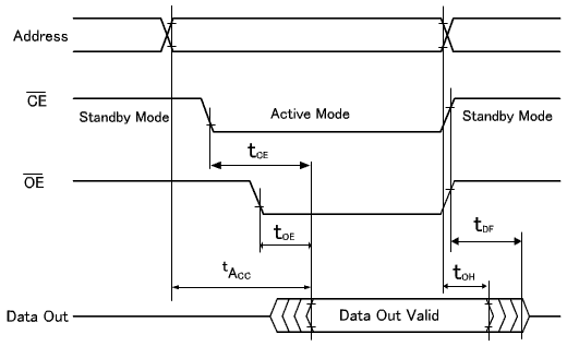
Read timing waveform Figure 13.7 shows the HN27C4001G read timing. Read data is output from an I/O pin when the access time (tACC), CE output delay time (tCE) and OE output delay time (tOE) are satisfied.
|