When connecting a CPU and a memory using a 16-bit data bus, use a pair of memories having 8 bits per address, or use a memory having 16 data pins. The example described here uses a pair of memories having 8 bits per address, which are connected as memories at even- and odd-numbered addresses, respectively.
To read/write 16-bit data, two addresses must be accessed simultaneously. It is impossible, however, to output two addresses to the address bus simultaneously. Remember that the upper digits of 16-bit data in the memory must be stored in an even-numbered address and the lower in an odd-numbered address (even-numbered address + 1). An "even-numbered address" and an "even-numbered address + 1" are the same from A23 to A1 in binary notation and only A0 differs. No problem arises if A0 is not used, since A1 to A23 are the same. A0 = 0 represents an even number and A0 = 1 an odd number. A combination of an "odd-numbered address" and an "odd-numbered address + 1 (even-numbered address)" does not make A1 to A23 the same, disabling access as 16-bit data. This situation is not limited to the H8/3048 but common to all 16-bit microcomputers.
HWR and LWR are used instead of the A0 signal. HWR = L represents 8-bit writing to an even-numbered address (A0 = 0) and LWR = L means that to an odd-numbered address (A0 = 1).
HWR = LWR = L means writing to both even- and odd-numbered addresses. Only the RD signal is used for reading by the CPU. During reading, data are always handled as 16 bits without distinguishing between 8- and 16-bit data. Sixteen bits are read even if the MOV.B instruction is used for reading from the memory. Non-used 8 bits are not read into the CPU although they are output from the memory. Reading data not required for the memory will not have a negative effect. For writing, however, 8- and 16-bit writing must be clearly distinguished since it changes the contents of the memory. This is shown in Table 13.10.
| Table 13.10: Reading/Writing on 16-bit Data Bus |
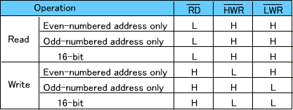 |
Figure 13.27 shows an example to connect the CPU and SRAMs using a 16-bit data bus.
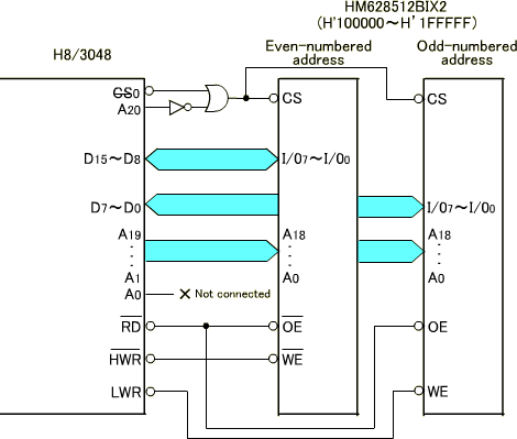 |
| Figure 13.27: Connection Between CPU and SRAMs (16-bit Data Bus) |
Address, CS and OE signals are commonly input to two memories. For the memory at an even-numbered address, HWR is input to the WE pin and the data pins are connected to the upper 8 bits of the CPU. As for the memory at an odd-numbered address, on the other hand, LWR is input to the WE pin and the data pins are connected to the lower 8 bits of the CPU.